![]()
![]()
![]()
![]()
![]()
![]()
![]()
![]()
![]()
![]()
![]()
Côté bricolage :
Une
interface
24 Inputs/Outputs
pour votre ZX81.

![]()
TIREZ PLUS DE VOTRE SINCLAIR
![]()
Mis à Jour : Juin 2007.
|
|
|
|
|
|
|
|
|
|
|
|
|
Côté bricolage : Une
interface |
||||||||||
|
|
TIREZ PLUS DE VOTRE SINCLAIR
|
|||||||||
|
Mis à Jour : Juin 2007. |
||||||||||
|
Kit
by Xavier Martin. - |
Electronic
Kit n°1 : |
|
||||||||||||
|
|
|
|||||||||||||
|
Centronics
Sub D 25 pins card.
Waring
:
(Components side using straps wiring)
Components side:
PCB: (époxy single side) (Copper side)
(
rear view of ZX – extension port at the left side) |
|
|||||||||||||
|
|
||||||||||||||
|
|
||||||||||||||
|
|
||||||||||||||
|
|
||||||||||||||
|
|
||||||||||||||
|
|
||||||||||||||
|
|
||||||||||||||
|
|
||||||||||||||
|
|
||||||||||||||
|
|
||||||||||||||
|
|
||||||||||||||
|
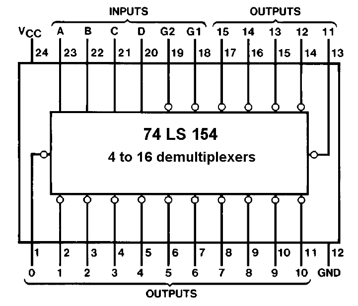
Wiring diagram :
If you had to initialize a new port, active if EXT1 is on, you had to poke at 0000h to active the Y0 on 74LS154 ship set.( list of offset addresses on the wiring diagram) It able to trig and initialize 15 extra ports devices. This bits could be used on other projects to ... active or valid a new device (active an IDE disk ... Disk C... Disk D...)
|
||||||||||||||
|
Ce montage est composé de : |
||||||||||||||
|
References |
components |
Q |
P.U. |
Price.(€) |
||||||||||
|
IC1 |
P.P.I – 8255A intel or compatible. |
1 |
- |
4,27 |
||||||||||
|
IC2a |
74LS245 : Latch IO Buffer |
1 |
- |
|
||||||||||
|
IC2b |
74LS245 : Latch IO Buffer |
1 |
- |
|
||||||||||
|
IC3 |
74LS154 : 4 to 16bits Multiplexer. |
1 |
- |
|
||||||||||
|
|
|
|
|
|
||||||||||
|
P1 |
Centronics SubD 25 pins socket for PCB. |
1 |
- |
|
||||||||||
|
ZX |
2x23 pins DF connector. |
1 |
- |
|
||||||||||
|
To E/S daughter cards. |
25x1 connector. |
|
|
|
||||||||||
|
|
Boîtier PCV (noir) |
1 |
- |
|
||||||||||
|
|
|
|
|
|
||||||||||
|
|
|
|
|
|
||||||||||
|
|
|
|
|
|
||||||||||
|
|
||||||||||||||
|
|
||||||||||||||
|
|
||||||||||||||
|
|
||||||||||||||
|
Utilisation: |
||||||||||||||
|
8255A contrôl register : Address 14339 / 3803h
|
||||||||||||||
|
D7 |
D6 |
D5 |
D4 |
D3 |
D2 |
D1 |
D0 |
|||||||
|
Flag |
Mode 1 |
Mode 2 |
Canal A |
Canal C |
Mode |
Canal B |
Canal C |
|||||||
|
D7:
0
= Mode Bit / Reset. D6 et D5:
00
= Mode 0 D4: Canal A
0
= Output D3: Canal C (PC4 à PC7)
0
= Output D2: Sélection du Mode.
0
= Mode 0 D1: Canal B
0
= Output D0: Canal C 0
= Output |
||||||||||||||
|
8255A setup :
PA
: Address 14336 / 3800h
PB
: Adresse 14337 / 3801h
PC
: Adresse 14338 / 3802h
Data Register: ( PA D0-7 bidirectional read and write)
Control
Register: ( PB D0-3 ouput mode)
|
||||||||||||||
|
|
||||||||||||||
|
Basic programs:
PA
port test (output):
PB
port test (output):
PC
port test (output):
PA
port test (input):
PA
port in input mode: |
||||||||||||||
|
|
||||||||||||||
|
|
||||||||||||||
|
|
||||||||||||||
|
|
||||||||||||||
|
Tips:
Pin 1 : Strobe. (Input)
Strob
is usualy set to high level; low level if case of datas
transfer.
|
||||||||||||||
|
Kit
n°2 : |
||||||||||||||
|
Implantation
: (XavSnap)
|
||||||||||||||
|
Upper
Connector to IDE device Components side:
|
||||||||||||||
|
PCB:
|
||||||||||||||
|
PBC
File: (XavSnap)
|
||||||||||||||
|
Driver and card emulation available on Vb81 XuR htt://zx81.vb81.free.fr
|
||||||||||||||
|
index #1:
Datasheet regard 8255 - http://www.datasheetcatalog.com pour le 8255A de Intel.
|
||||||||||||||
|
index #2:
|
||||||||||||||
|
Index #3:
|
||||||||||||||
|
|
||||||||||||||
|
|
||||||||||||||
|
|
||||||||||||||
|
|
||||||||||||||
|
|
||||||||||||||